Structured Digital Design Lab
This class was the 2nd semester of digital design; a followup to "Digital Design Lab." In Structured Digital Design we took a programmatic approach to our design, simulation, and testing of digital circuits using VHDL. VHDL stands for VHSIC Hardware Description Language where VHSIC is the name of the US government program that developed it. A hardware description language is a specialized language that describes the structure and behavior of digital logic circuits and gives us the power to design much more complex circuits. All of the projects in this course were written in VHDL and simulated using ModelSim.
Labs
With these labs, we designed circuits by writing VHDL code entities and describing their behavior in the entity's architecture. In the real-world VHDL files can be read by a logic synthesizer that turns the code into a digital logic circuit. In this course we tested our VHDL entities in ModelSim by simulating input signals and observing the output.
-
Lab 1 - 1-bit Full Adder (Behavioral Method)
Report
CodeAn introduction to VHDL. With this lab we described a simple 1-bit full adder as a VHDL entity using the behavioral method. This means we defined the adder's input and output ports and used logical VHDL statements to describe the behavior we want our adder to perform. This allows a synthesizer to design the circuit itself to achieve our desired behavior.
An example synthesized logic circuit for a 1-bit full adder 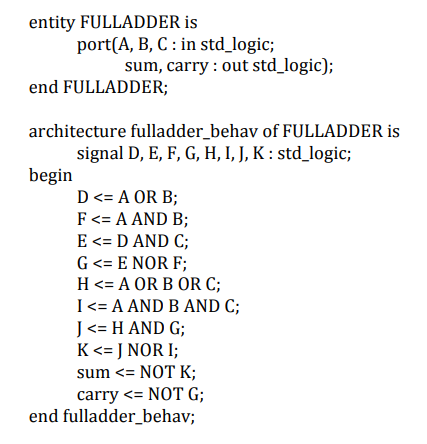
The architecture of a behavioral full adder describing its behavior; the actual circuit determined by the synthesizer -
Lab 2 - 1-bit Full Adder (Structural Method)
Report
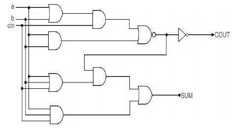
CodeWe designed the same adder from lab 1 using the structural method. By comparison, rather than allowing the synthesizer to design our circuit, we defined entities to represent logic gates and specified exactly how we want our circuit to look.
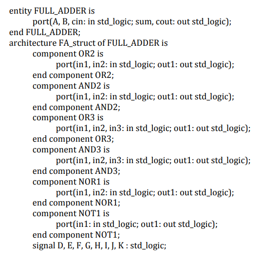
The architecture of a structural full adder using components to describe the digital circuit 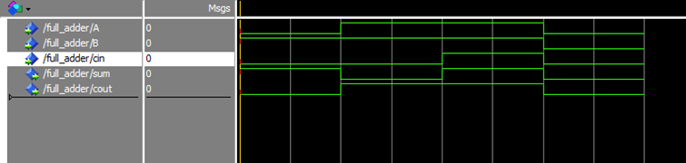
Testing our structural full adder; initially 02 and 12 are added with no carry in to produce a sum of 12 with no carry out -
Lab 3 - 4-bit Register and Tri-State Buffer
Report
CodeWe designed two slightly more complex circuits - a 4-bit register and 4-bit tri-state buffer. A register is a synchronous component that holds memory and input/outputs it on a clock cycle. A tri-state buffer is a register that adds the ability to "hold" its data and only output it when specified. We designed these using the behavioral method.
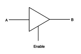
A single-bit tri-state buffer takes an input A and outputs it to B when the enable bit is set 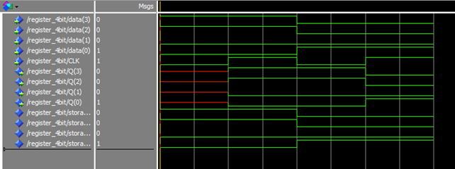
Testing the register; I initially load the register with 11002 in the data lines and observe it output in the Q lines on the clock signal 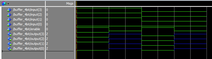
Testing the tri-state buffer; I initially load the input with 11102 and observe it move to to the output when enable is set to 02 -
Lab 4 - 16-bit Calculator
Report
CodeI designed a 16-bit calculator and simulated it both in ModelSim and on an Altera DE-2 programmable logic board. This calculator is able to perform addition, subtraction, and some boolean algebra. The design calls for an output bus of one nibble (half a byte or 4 bits) meaning only 4 bits may be sent to the output at once. To accomplish this four 4-bit registers and tri-state buffers are used to store the result and allow the user to choose which nibble will be sent to the output. In this design both behavioral and structural components are used.
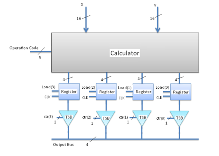
The top level diagram; the calculator kernel performs the calculation and the registers and tri-state buffers push the result to the output 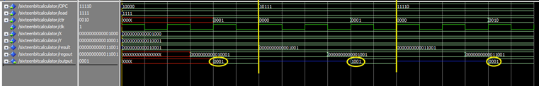
Testing the calculator in ModelSim; in simulation 2 X (10002 or 8) is subtracted from Y (100012 or 17) and produces the result (10012 or 9) in the output 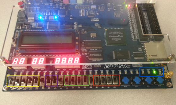
Testing the calculator on the board; yellow switches are the operation code, green and red switches represent the two inputs X and Y, and blue LEDs represent the output; I had to scale the calculator down to 4 bits to fit on the board Demo on the programmable logic board
First calculation shows 00012 + 00012 = 00102 (1 + 1 = 2)
Second calculation shows 00112 + 00112 = 01102 (3 + 3 = 6)
Third calculation shows 00112 - 00012 = 00102 (3 - 1 = 2)
Fourth calculation shows 00012 - 00102 = 11112 (1 - 2 = -1) using 2's complement
Projects
-
Arithmetic Logic Unit (ALU)
Report
CodeAn ALU is a core component of virtually every processor. It performs arithmetic and bitwise operations on binary numbers. Our ALU is 16 bits and supports 16 operations including additions, subtractions, and 5 logical operations. It outputs a 16-bit result as well as 6 status codes.
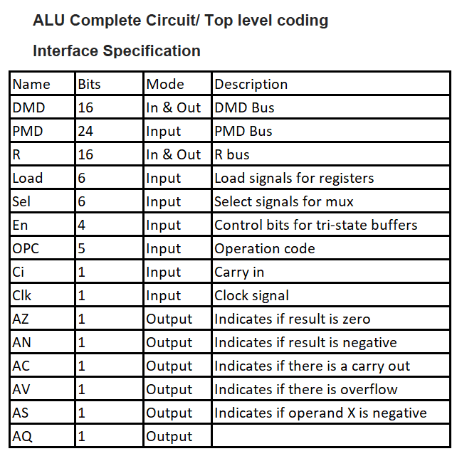
The specification for our ALU's inputs and outputs 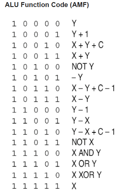
The operations our ALU can perform and their associated opcodes 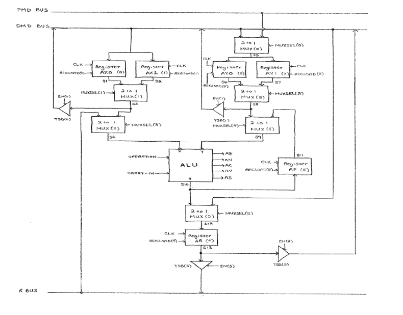
The design synthesis of our ALU 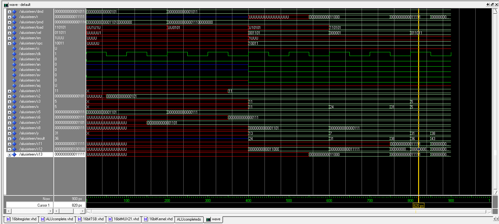
Testing our ALU with 3 calculations -
Multiplier Accumulator (MAC)
Report
Code
PresentationThe multiply-accumulate unit is a widely-used circuit whose function is to perform multiplication on two numbers and add that product to an accumulator. This function is crucial to performing convolution and the Fast Fourier Transform (FFT), common algorithms in digital signal processors. Our MAC unit is 16 bits and is also capable of performing multiplication with cumulative subtraction as well as single-cycle multiplication.
We designed all of the components of our circuit behaviorally and then designed our top-level circuit structurally using these components. We tested the circuit on ModelSim and also downloaded the two main components - the multiplier and add/subtract component - onto an Altera programmable logic board to visualize our results. Like before, we had to scale down the components to 4 bits to fit on the board.
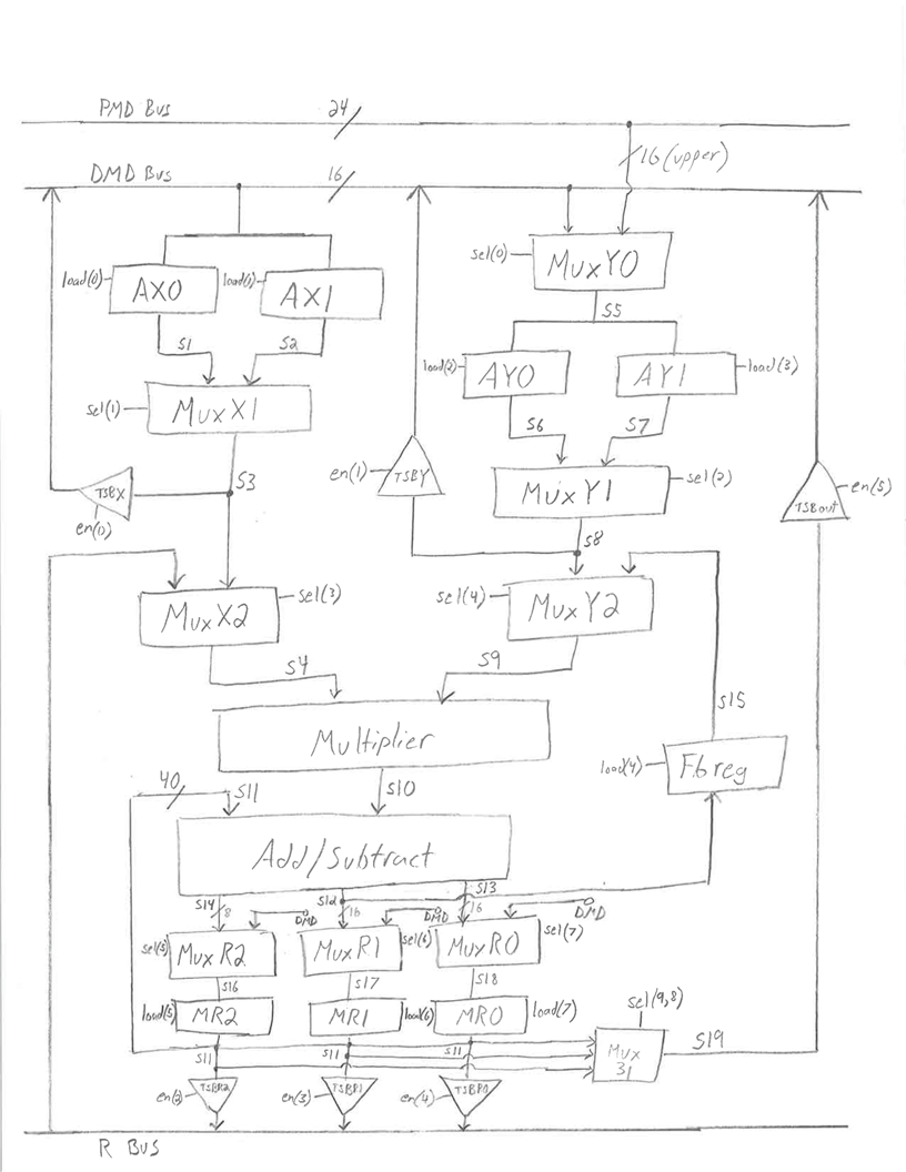
The design synthesis of our MAC unit 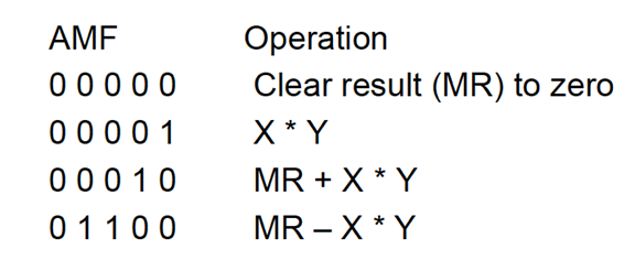
The operations our MAC unit can perform with their associated opcodes 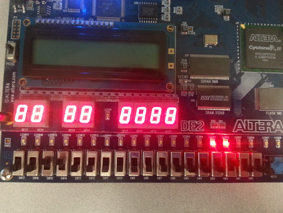
Testing the multiplier on the logic board; the operands are set by the switches and the result shown with red LEDs
This example shows 00112 x 00102 = 11002 (3 x 4 = 12)