Digital Design Lab
A study of boolean algebra, digital circuits, and logic gates. Our labs and projects involved designing various digital circuits using combinatorial and sequential logic design and then testing them on a breadboard using integrated circuits.
Labs
-
Lab 1 - 7-Segment Display and Sequence Detector
ReportIn this lab we learned the difference between combinatorial and sequential logic design by designing both a 7-segment display (combinatorial) and a sequence detector (sequential). A 7-segment display is a common circuit that uses 7 separate LEDs to represent a single decimal digit. The sequence detector circuit will light up a single LED when a specified combination of numbers is entered on the seven-segment display. To design both we had to derive output equations that relate a binary input to our specified outputs.
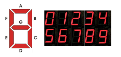
A 7-segment display showing the 7 LED outputs (a-g) 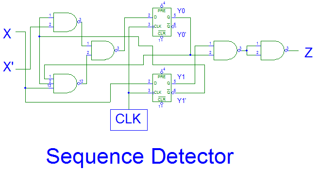
The circuit for our sequence detector using NAND gates and flip-flops -
Lab 2 - 3-bit Synchronous Counter
ReportWe designed a counter circuit that can be loaded with a starting number and set to count up or down in the range of 0-7. The circuit uses the 7-segment display from the previous lab to display the numbers. This lab demonstrated the transition to medium-scale integration (MSI) technology through the use of the multiplexer. MSI circuits use chips that contain hundreds of transistors each rather than only a few and greatly expanded the capabilities of digital circuits.
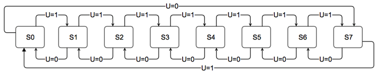
The next state diagram used in the design of the counter showing the 8 possible output states representing the numbers 0-7 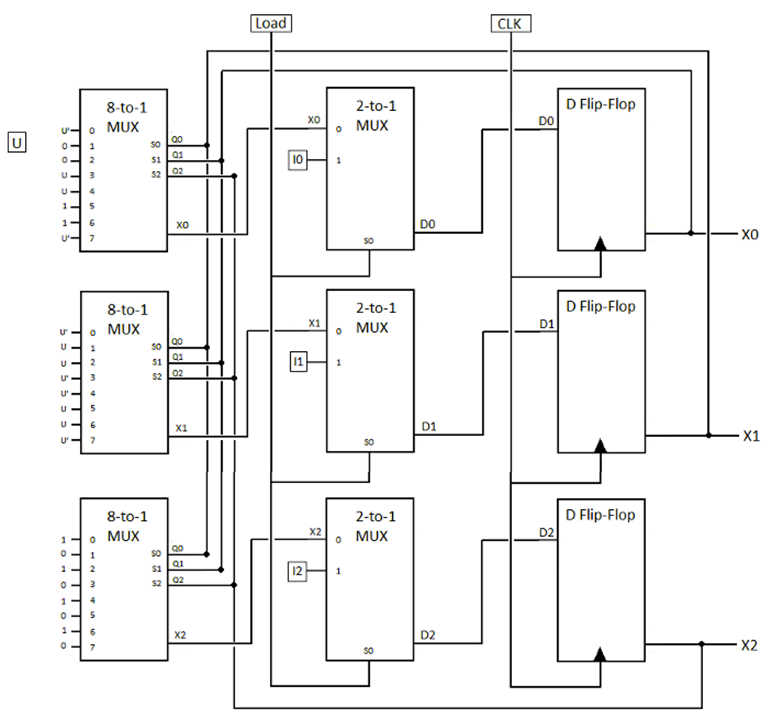
The complete logic diagram for our counter showing the use of multiplexers -
Lab 3 - Tone Generator
ReportIn this lab we generated a sequence of audible tones and played them through a speaker. To do this we designed a sequence generator to cycle through 13 different tones and a frequency generator to create the audible frequency. The frequency generator uses a timer IC to generate a 16kHz base frequency and a counter to divide the frequency for each tone. The final frequency signal is sent to a speaker.
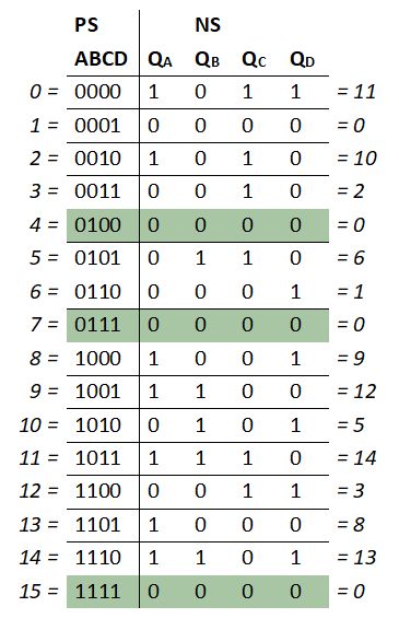
The next state table used in the design of the sequence generator, each state is represented by 4 binary bits 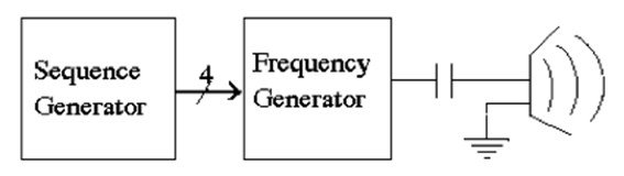
The top level diagram for our tone generator 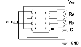
The connection diagram of the 555 timer IC used to generate the frequency 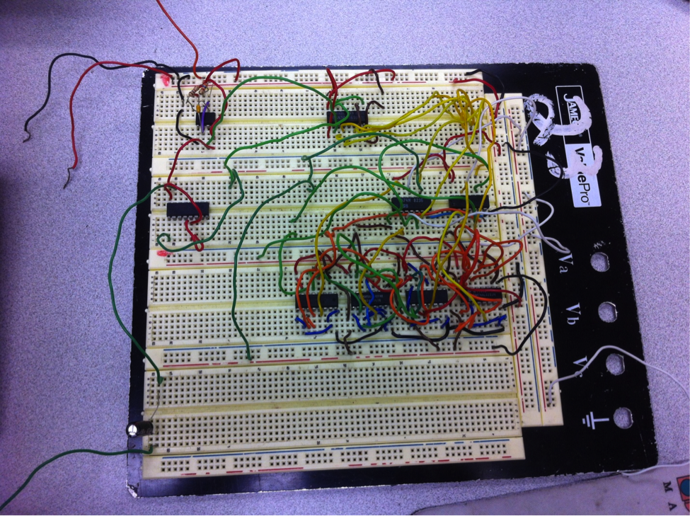
Our final circuit on the breadboard; the timer IC can be seen in the top left, speaker not visible
Projects
-
Shift Register and Signature Analyzer
ReportWe designed a shift register and used that to build a signature analyzer. A register is a component that holds memory and a shift register "shifts" the data in its memory in a binary stream to its output at every clock cycle. When modified we can turn a shift register into a pseudo-random binary sequence generator. This is a fancy term to describe a device that takes a long binary number as its input and uses it to output a smaller, random binary number. This will be our signature generator - the long binary input is data and the randomly generated output is that data's unique signature.
Signature analyzers are commonly used to test that other digital circuits are working correctly by verifying that the correct sequence of bits is flowing through certain points in the circuit. Our signature analyzer design was simulated using Altera Quartus.
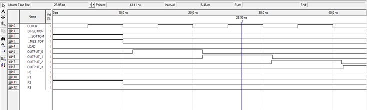
Testing the shift register; here I perform a right shift by loading data in P2 and observing it shift through the outputs at each clock cycle 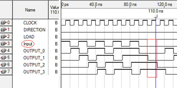
Testing the signature analyzer; the input sequence entered is 1010101010 shown on the input row and the resulting signature is displayed by the outputs in the red box (0011) 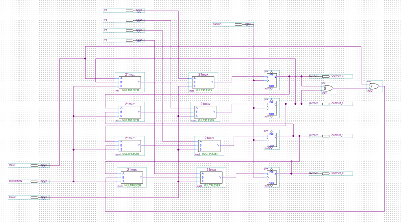
Our final logic diagram for the signature analyzer -
4-bit Multiplier
Report
PresentationA multiplier is a common circuit and a core component of the Arithmetic Logic Unit (ALU) found in every CPU and most microprocessors. The multipiler circuit we designed was a 4-bit by 4-bit multiplier and used the add-and-shift algorithm. This algorithm required us to use full adders and shift registers in our design. Our multiplier was simulated in Altera Quartus and also implmented on Altera UP2 programmable logic board.
The add-and-shift algorithm performs binary multiplication on two N-bit numbers in O(N)=2N operations 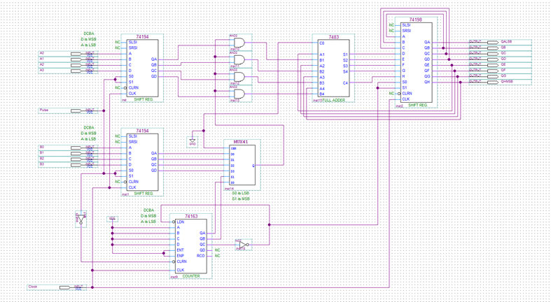
Our final logic diagram for the 4-bit multiplier 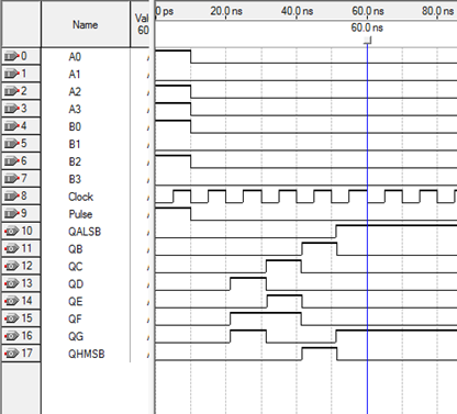
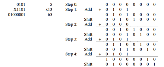
Testing the multiplier; the two numbers being multiplied are shown in A (11012 or 13) and B (01012 or 5) and the result is shown in Q (010000012 or 65) 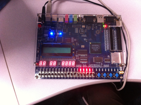
The multiplier being tested on the programmable logic board; the switches on the bottom are set with the arguments (10 and 3) and the LEDs show the result (111102 or 30)